25+ fsk transmitter and receiver circuit diagram
Here the circuit diagram of laser transmitter. A laser diode LD1 with maximum operating voltage of about 26V DC and maximum operating current of 45 mA is applied to transmit the.
Phase Shift Keying Types Advantages Disadvantages And Applications
The ADF7020-1 uses an external VCO inductor.
. The primary fiber optic receiver circuit diagram can be seen in the upper section of the below diagram the output filter circuit is drawn. A power supply is provided for the oscillator and the final power amplifier. For this a potentiometer is used but it was not working.
SYMBOL PARAMETER CONDITIONS MIN. I wont be able to help you contructing them or give more info than what is written on this page. That it is synchronized with the transmitter.
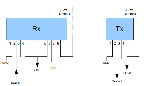
The entire fiber optic transmitter circuit diagram can be seen below. The receiver circuit is the most simplest ever madeIt is making use of radio diode rather than any inductorWe are not using any tuning circuit hereThe ic used here is a high gain. It detects the transmitted 40kHz signal which is amplified by the amplifier built around.
Download scientific diagram QPSK Transmitter and Receiver from publication. You will find many integrated circuits suitable to work like VCO along with many other configurations built using discrete parts. Frequency Shift Keying FSKAmplitude Shift Keying ASK receiver UAA3220TS DC CHARACTERISTICS VCC 27 V.
For application diagram see Figs 9 and 10. Set up a QFSK link with a data rate of 2Kbps and a frequency separation of 8KHz a. Design and Implementation of SDR Transceiver Architecture on FPGA Usage of Software-Defined Radio.
A block diagram representing various stages of a basic continuous wave radio transmitter. UNIT Supplies VCC supply voltage 27 55 V ICC supply current operating mode on. The ADF7020-1 is a low power highly integrated FSKGFSK ASKOOKGOOK transceiver designed for operation in the low UHF and VHF bands.
Verify the spectrum at the receiver is as expected. Firstly a 38 kHz IR transmitter circuit is used for which you had to design an astable to generate that frequency. The purpose of this page is to make the circuit diagrams available for educational purposes.
The receivers transducer unit RX is kept near the ultrasonic transmitter under test. 2FSKQPSKTransmitterandReceiverDesignand Performance by NelsAFrostenson.
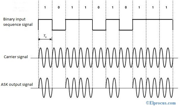
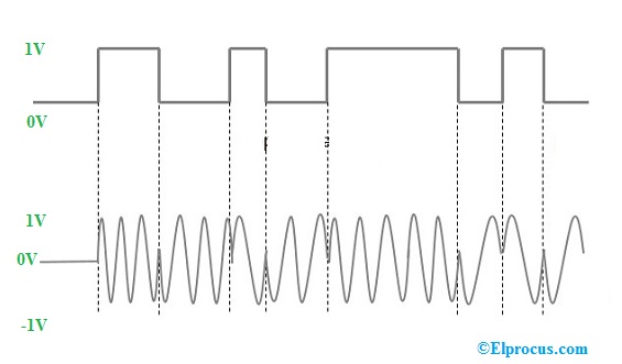
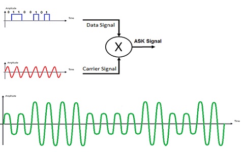
Amplitude Shift Keying Circuit Diagram Working And Its Applications
Rf Communication Protocols And Its Applications
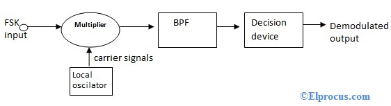
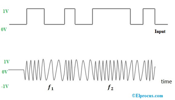
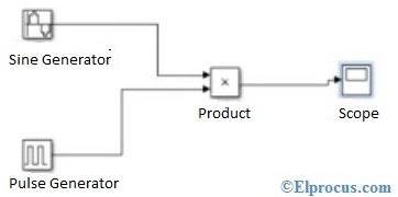
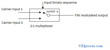
Frequency Shift Keying Fsk Working Advantages And Disadvantages
Digital Modulation Types And Differences Between Analog And Digital
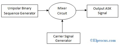
Amplitude Shift Keying Circuit Diagram Working And Its Applications
Amplitude Shift Keying Circuit Diagram Working And Its Applications
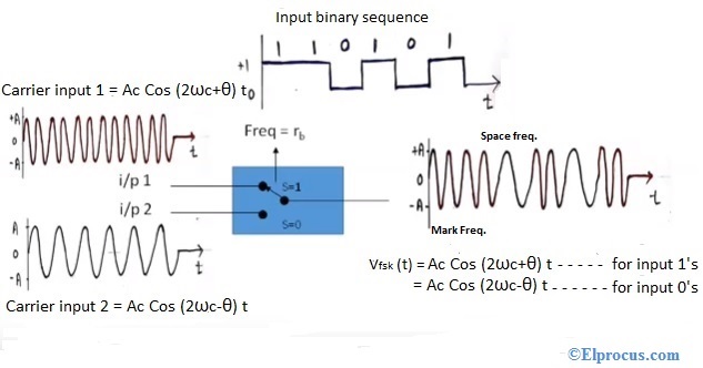
Frequency Shift Keying Fsk Working Advantages And Disadvantages
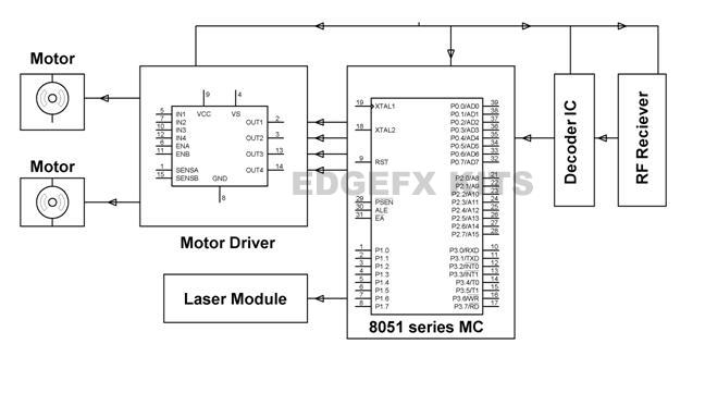
Rf Communication Protocal For Industrial And Home Applications
Amplitude Shift Keying Circuit Diagram Working And Its Applications
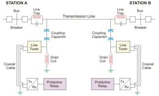
Power Line Carrier Communication Circuit Diagram And Its Working
Frequency Shift Keying Fsk Working Advantages And Disadvantages
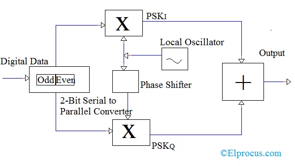
Quadrature Phase Shift Keying Circuit Diagram Advantages
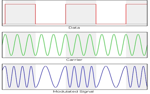
Frequency Shift Keying Fsk Working Advantages And Disadvantages
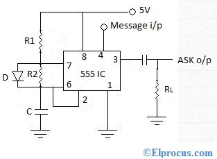
Amplitude Shift Keying Circuit Diagram Working And Its Applications
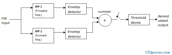
Frequency Shift Keying Fsk Working Advantages And Disadvantages
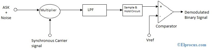
Amplitude Shift Keying Circuit Diagram Working And Its Applications
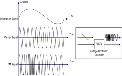
Frequency Modulation Modulation Index Bandwidth Applications